SNAP - Swiss National Applicationlab for Photonics
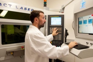
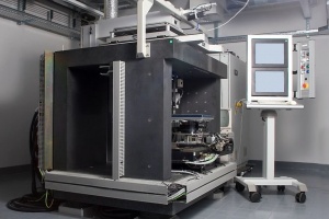
The SNAP cluster combines institues working on laser beam material processing and offers test beds and application labs for Swiss companies developing new laser beam sources for material processing. It recommends the best suitable institute, the best approach and supports implementation. The involved institutes give the SME assistance for Innosuisse projects if technology development is needed to solve the problem.
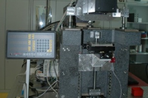
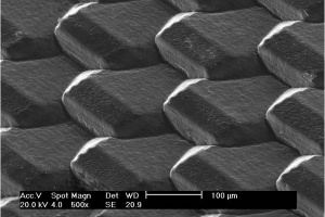
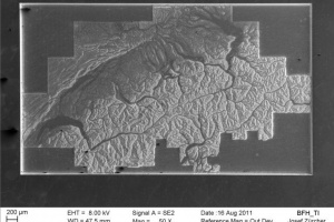
Laser beam material processing covers
SNAP conducts one tutorial seminar at the yearly EPMT trade-show in Geneva and holds several workshops per year on the latest progress to advance the laser machining technology and tools.
Laser beam material processing covers
- Laser micromachining and drilling of almost any material, i.e. metals, textiles, tissue, ceramics, glass, plastic and carbon composites
- Functional structures on surfaces
- Laser welding, soldering and brazing
- 3D-Laser surface treatment of many materials (polishing, hardening, structuring, marking, engraving,)
- Rapid manufacturing, 3D printing
SNAP conducts one tutorial seminar at the yearly EPMT trade-show in Geneva and holds several workshops per year on the latest progress to advance the laser machining technology and tools.
Contact
Dr. Andreas Burn
andreas.burn@sipbb.ch
+41 32 530 88 48
SIPBB
Switzerland Innovation Park Biel/Bienne
Aarbergstrasse 46
2503 Biel - Bienne BE
andreas.burn@sipbb.ch
+41 32 530 88 48
SIPBB
Switzerland Innovation Park Biel/Bienne
Aarbergstrasse 46
2503 Biel - Bienne BE