Quantitative CMOS Imaging
Wed, 19.05.2021, online
Quantitative CMOS Imaging – qCMOS:
The Dawn of a New Era
Hamamatsu Photonics will introduce the latest photon-resolving quantitative CMOS imaging technology qCMOS which will provide you an overview of the incredible benefits of semiconductor image sensors.Imaging in general and semiconductor imaging in particular have penetrated every aspect of our lives, especially in the sciences. They have empowered many experiments from relying on subjective recording into objectively documentable, repeatable, and quantifiable methods. The evolution of imaging technology is directly linked to new scientific achievements. Demanding and extremely valuable techniques such as single-molecule-based methods would not be possible without appropriate image sensors. Conceptually, all imaging procedures have to find their optimum trade-off between resolution, sensitivity, and speed. While the theoretical basis of this challenge lies within the physical foundations of imaging with discrete entities — that is, photons — technological limitations exacerbate this difficulty.
The incessant progress of CMOS technology has made it possible to continuously minimize transistor size, to reduce dark current effects, and to decrease electronic readout noise. Today, we find ourselves at the dawn of a new era. The novel quantitative CMOS qCMOS technology finally reaches the physical limit: reliable quantification of photon numbers within each pixel, eliminating the influence of technology on the triangle of frustration (resolution, sensitivity, speed). To set the stage for the release of groundbreaking products in the near future, Hamamatsu would like to invite you to a review of the history of semiconductor image sensors, based on the relentless advances of semiconductor technology, culminating in photon-resolving quantitative imaging — qCMOS!
Who should attend:
R&D scientists, engineers, Q/C professionals, educators, and others involved in the use, purchase, or maintenance of CMOS imaging systems. This webinar is for a wide range of experience levels, providing technical details on semiconductor image sensors old and new, as well as educating those interested in learning the latest in CMOS technologies.
Speaker
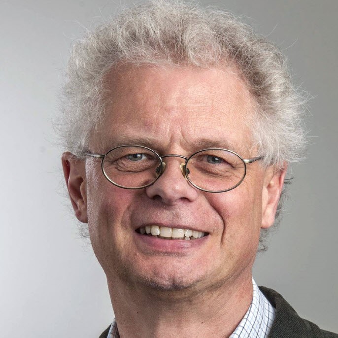
Peter Seitz, Ph.D., studied physics and earned his master degree in solid-state/semiconductor physics at ETH Zurich. His Ph.D. thesis at ETH was on 2D and 3D x-ray imaging and computed tomography. He subsequently worked for RCA, General Electric, the Paul Scherrer Institute, CSEM, the University of Neuchatel, and the two Swiss Federal Institutes of Technology, ETH and EPFL. Today, Seitz is senior technologist at Hamamatsu Photonics Europe, an adjunct professor emeritus of opto-electronics at EPFL, and a startup coach at the Innovation and Entrepreneurship Lab of ETH. He is also active as a member of the Executive Committee of the European Technology Platform Photonics21 and as vice president of the Swiss Academy of Engineering Sciences SATW. He is also a member of the Scientific Advisory Board of the Werner Siemens Foundation.
Date
Wednesday, 19 May 2021
Time
5.00 pm - 6:00 PM CEST
Registration
Contact Hamamatsu Photonics France - Swiss Office
Prof. Dr. Peter Seitz
Contact Swissphotonics
Dr. Christian Bosshard
Managing director Swissphotonics
+41 61 690 60 40
30 April 2021, Beni Muller + Iris Bollinger